BPI IO extend module
Contents
Product Overview
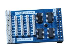
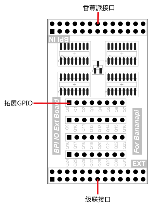
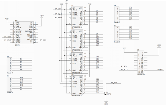
This module is designed specifically for the Banana Pi IO expansion modules, which can effectively solve the banana send IO port insufficient. Module uses four 74HC595 chips to expand 32 IO ports. As shown above, the top of the module will expand the IO of Banana Pi again that can be cascaded for more IO expansion modules can theoretically unlimited expansion.
Product Features
- 1. Expanded 32 GPIO
- 2. Infinity connection for the same module
- 3. Use wiringPi API ,sample code
Port
- 1. Banana Pi 2X13 port
- 2. Banana Pi 2X13 cascade port
- 3. Q0-Q31 expanded IO port
Product Parameters
- 1. Working voltage: 2.4V-5V
- 2. IO voltage: 3.3V
- 3. Expanded 32 unidirectional IO
- 4. Connection through SPI
- 5. 100 MHz (typical) shift out frequency
- 6. 8-bit serial input
- 7. 8-bit serial or parallel output
- 8. Specified from -40C to +85C and from -40C to +125C
Typical Application
- 1. Drive the lattice screen
- 2. Driver numeric display
- 3. Drive matrix LED
Product Specification
How to Use
Insert the module that the silk screen says “BPI IN”. Pay attention don’t make the direction reversed! The correct direction of insert module is above the Banana Pi’s PCB; The 8*4header in the module are Q0-Q31 expanded GPIO, they can connect to the peripheral through the Dupont Line. The header which near silk screen write ”EXT” expand GPIO of Banana Pi, user can cascade the other module or the same module.
More information
The 74HC595; 74HCT595 are high-speed Si-gate CMOS devices and are pin compatible with Low-power Schottky TTL (LSTTL). They are specified in compliance with JEDEC standard No. 7A.
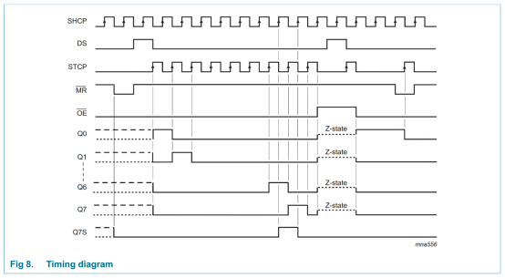
The 74HC595; 74HCT595 are 8-stage serial shift registers with a storage register and 3-state outputs. The registers have separate clocks.Data is shifted on the positive-going transitions of the shift register clock input (SHCP). The data in each register is transferred to the storage register on a positive-going transition of the storage register clock input (STCP). If both clocks are connected together, the shift register will always be one clock pulse ahead of the storage register.
The shift register has a serial input (DS) and a serial standard output (Q7S) for cascading. It is also provided with asynchronous reset (active LOW) for all 8 shift register stages. The storage register has 8 parallel 3-state bus driver outputs. Data in the storage register appears at the output whenever the output enable input (OE) is LOW.
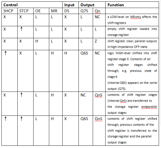
Function table
- H = HIGH voltage state;
- L = LOW voltage state;
- ↑= LOW-to-HIGH transition;
- X = don’t care;
- NC = no change;
- Z = high-impedance OFF-state.
Timing diagram
Schematic diagram
- More information please check:
http://www.nxp.com/products/logic/shift_registers/series/74HC_T_595.html
Example and test code
#include <wiringPi.h>
#include <stdio.h>
int SER = 12;
int RCLK = 10;
int SRCLK = 14;
unsigned char LED[8]={0x01, 0x02, 0x04, 0x08, 0x10, 0x20, 0x40, 0x80};
void SIPO(unsigned char byte);
void pulse(int pin);
void init() {
pinMode(SER, OUTPUT);
pinMode(RCLK, OUTPUT);
pinMode(SRCLK, OUTPUT);
digitalWrite(SER, 0);
digitalWrite(SRCLK, 0);
digitalWrite(RCLK, 0);
}
void delayMS(int x) {
usleep(x * 1000);
}
int main (void)
{
if (-1 == wiringPiSetup()) {
printf("Setup wiringPi failed!");
return 1;
}
init();
int i;
while(1) {
for(i = 0; i < 8; i++)
{
SIPO(LED[i]);
pulse(RCLK);
delayMS(50);
printf(" i = %d", i);
}
printf("\n");
delayMS(500); // 500 ms
for(i = 7; i >= 0; i--)
{
SIPO(LED[i]);
pulse(RCLK);
delayMS(50);
printf(" i = %d", i);
}
delayMS(500); // 500 ms
}
usleep(1000);
digitalWrite(RCLK, 1);
}
void SIPO(unsigned char byte)
{
int i;
for (i=0;i<8;i++)
{
digitalWrite(SER,((byte & (0x80 >> i)) > 0));
pulse(SRCLK);
}
}
void pulse(int pin)
{
digitalWrite(pin, 1);
digitalWrite(pin, 0);
}
